
基于FPGA的高精度震荡信号源的设计
基于FPGA的高精度震荡信号源的设计(任务书,开题报告,外文翻译,论文11500字)
摘 要
信号发生器又称为波形发生器,是一种常用的信号源,广泛应用于电子电路、通信、控制和教学实验等领域。它是科研及工程实践中最重要的仪器之一,以往多用硬件组成,系统结构比较复杂,可维护性和可操作性不佳。随者计算机技术的发展,信号发生器的设计制作越来越多的使用计算机技术,种类繁多,价格、性能差异很大。用FPGA或CPLD来实现,它的优点是可以进行功能仿真,而且FPGA和CPLD的片内资源丰富,设计的流程简单。
本课题主要研究基于FPGA的高精度震荡信号源的设计和实现,设计研究工作大部分是在计算机软件平台Quartus II下完成的。在Quartus II环境下,先用Verilog语言进行各模块的程序编写,然后生成顶层模块,连接各模块端口,形成信号发生器顶层原理图,通过Quartus II仿真,得到具体数据。最后通过FPGA开发板连接示波器,调试出波形进行总结和分析。
关键词:FPGA;Verilog编程语言;信号发生器;Quartus II
Abstract
Signal generator, also known as a waveform generator, is a common source, widely used in electronic circuits, communication,control,and teaching experiments.It is one often most important instrument in the research and engineering practice, past use of hardware components, system architecture is more complex, poor maintainability and operability. With the development of computer technology, more and more, signa1 generator design is the use of computer technology, a wide range of price, performance, very different. FPGA or CPLD, its advantage is that the functional simulation, and FPGA and CPLD chip is rich in resources, the design process is simple.
[资料来源:http://doc163.com]
The main subject of study design and implementation of FPGA-based signal generator,designed most of the work completed in the computer software platform, the Quartus II, The programming of the module in the Quartus II environment, use the verilog language and then generate a top-level module, connect the ports of each module, the formation of the top-level schematic diagram of the signal generator by the Quartus II simulation specific data. Finally, the FPGA development board connected to the oscilloscope, debugging, waveform were summarized and analyzed.
Key words:FPGA;Verilog programming language;signal generator;Quartus II
[来源:http://www.doc163.com]
目录
摘要 Ⅰ
第一章 绪论 1
1.1 研究的目的及意义 1
1.2 信号发生器的发展状况 2
1.3 主要研究的基本内容及目标 3
1.4 小结 3
第二章 FPGA简介 4
2.1 FPGA概述 4
2.2 FPGA基本结构 4
2.3 FPGA系统设计流程 6
2.4 FPGA开发编程原理 8
2.4 小结 9
第三章 信号源总体设计方案 10 [资料来源:Doc163.com]
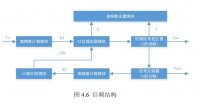
3.1 信号源的构成 10
3.2 信号源的工作原理 10
3.3 小结 11
第四章 单元模块设计与实现 12
4.1 锁相环模块的设计与实现 12
4.1.1 锁相环的数学模型 12
4.1.2 Quartus II中的的锁相环 13
4.2 分频器模块的设计与实现 16
4.2.1 分频器的工作原理 16
4.2.2 Quartus II中的分频器 17
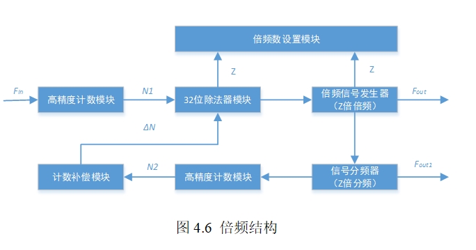
4.3 倍频器模块的设计与实现 19
4.3.1 倍频器的工作原理 19
4.4 整体功能的设计与实现 20
4.4.1 无倍频模块 20
4.4.2 有倍频模块 22
4.5小结 23
第五章 总结与展望 24
参考文献 25
致谢 26