
基于FPGA和DS1302芯片的数字电子表的设计
基于FPGA和DS1302芯片的数字电子表的设计(任务书,开题报告,外文翻译,论文10600字)
摘 要
本文设计一个基于FPGA和DS1302芯片的多功能数字钟,用数码管显示时间。 本设计采用EDA技术,以硬件描述语言Verilog HDL为系统逻辑描述语言设计文件,使用了Quartus11作为编程软件。采用了自顶向下的设计方式,各个模块功能清晰,易于修改及扩展功能。
系统由消抖模块、分频模块、功能模块、显示以及组成。共用8个数码管来显示结果,在仿真的时候,各个按键都能正常工作,并且输出的数值符合我们的预计,然后在开发板上进行调试,本设计能够完成时、分、秒、星期的分别显示等要求,当我们按下按键,数码管都会正常的显示我们需要的数据。具有调整时间,整点报时、闹钟功能。经仿真及实物验证,这次设计能满足需求,并且完成了预定的所有功能。
关键词:DS1302,Verilog HDL,FPGA
Abstract
In this article, a design based on the FPGA and DS1302 chip multifunction digital clock, 24-hour cycle; proofreading. This design uses EDA technology and hardware description language Verilog HDL logic description language for the system design documents in the Quartus11 tool software environment, using top-down design methodology, work together to build an FPGA-based digital clock by each basic module. [资料来源:http://Doc163.com]
System consists elimination buffeting module, frequency module, function modules, displays and components. Compiled and designed simulation program on a programmable logic device download validation, when this system is able to complete the hours, minutes and seconds are displayed, press calibration, the whole point timekeeping, alarm clock function..According to the simulation and actual object,it works well.
Key Words:DS1302,Verilog HDL,FPGA

目 录
第1章 绪论 1
1.1 选题意义与研究现状 1
1.2 国内外研究及趋势 1
第2章 软件及语言介绍 3
2.1 Quartus II介绍 3
2.2 Verilog介绍 4
第3章 芯片布置及介绍 6
3.1 总芯片设计 6
3.2 DS1302芯片 6
3.3 FPGA芯片 9
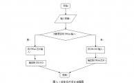
第4章 模块设计 12
4.1 分频模块 12
[来源:http://Doc163.com]
4.2 消抖模块 13
4.3 功能转换 14
4.4 数码管设计 15
4.5 硬件设计 18
第5章 仿真及实物结果 21
第6章 总结 27
参考文献 28
致 谢 29
[资料来源:http://www.doc163.com]