
触发器 FLIP-FLOPS
触发器 FLIP-FLOPS(中文4500字,英文3000字)
1简介
本文,我们将介绍如何设计可作为一位存储单元的触发器。触发器也可称为锁存器。采用触发器的逻辑电路结构其当前的输出是电路的前一稳定状态和当前稳定状态的函数。这样的电路称为时序逻辑电路。
所有的触发器都遵循同一规则:正反馈用来生成双稳态电路,双稳态电路是一个具有两个稳定工作点的电路。电路所处的工作点称为电路的一个状态。如果其状态能够读出和改变,那么此电路就可以作为一个一位存储器单元。
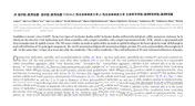
最简单的双稳态电路是在一个回路中利用两个反相器构成的。如图1-1所示。这个电路只有两个节点,A和B。由于是反相器,所以如果A是高电平,那么B就必须是低电平,或者反相。因此,电路具有两个稳定状态。
FLIP-FLOPS
1 Intorduce
In this passage, we show how to design flip-flops, which operate as one-bit memory cells. Flip-flops are also called latches. Logic circuits constructed using flip-flops can have the present output be a function of both the past and present inputs. Such circuits are called senfiential logic circuits.
All flip-flops are based on the same principle: Positive feedback is used to produce a circuit that is bistable . A bistable circuit is one that has two stable operating points. Which operating point the circuit is in is called the state of the circuit. If the state can be sensed and changed, then the circuit can function as a one-bit memory element.
The simplest bistable circuit is constructed using two inverters in a loop as shown in Figure 1-1.This circuit only has two nodes, A and B. Because of the inverters, if A is high, B must be low and vice versa; hence, the circuit has two stable states.
[资料来源:http://doc163.com]