
移相全桥DC-DC变换器的设计与研究
移相全桥DC-DC变换器的设计与研究(任务书,开题报告,外文翻译,论文17000字)
摘 要
随着国民经济的飞速发展,高质量电源的需求与日俱增,人们对其重量、体积、可靠性以及效率等各项性能指标的要求也越来越高。由于移相全桥DC-DC变换器具有结构简单、输出功率大、效率高、易于实现软开关、功率开关管所承受的电压电流应力小等一系列优点,其在中大功率的场合中得到了广泛的应用。因此对移相全桥变换器的研究具有十分重要的意义。
本论文研究了以全桥变换器作为主电路拓扑、以移相控制方式的移相全桥DC-DC变换器,该变换器的输入电压为300VDC,输出电压为20VDC,输出功率为500W,输出电压纹波不大于输出电压的10%。本文从电路拓扑的选择,控制方案入手,通过对参数的理论计算以及开闭环的仿真,设计了该变换器。
首先,论文阐释了移相全桥DC-DC变换器的意义,分析了变换器的工作原理,同时对开关功率管的缓冲环节和移相全桥DC-DC变换器中的变压器环节进行了研究。
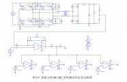
其次,对移相全桥变换器的主电路参数进行了设计,其中主要包括:高频变压器、功率开关管MOSFET、谐振电感。输出滤波电感、输出滤波电容、隔直电容等。
最后,本文介绍了SABER仿真软件,并且利用SABER软件对设计的变换器主电路分别进行了开环及闭环的仿真验证,给出了相应的图像。 [资料来源:http://Doc163.com]
关键词:DC-DC变换器 移相全桥 零电压开关 辅助谐振
The Design and Research of Phase-shifted Full-bridge DC-DC Converter
Abstruct
With the rapid development of national economy, the demand of high quailty power supply is almost in everywhere, peoples’ requirement for the power’s performance, such as its weight, volume, reliability and efficiency, is becoming harsher. As phase-shifted full bridge DC-DC converter has a simple structure, high output power and efficiency with its ability for soft-switching., the converter has been used in a wide range of applications. Therefore, it’s significant for us to study phase-shifted full-bridge converter
This paper studies a DC-DC converter based on full bridge inverter and phase shifting control tactics. The converter input voltage is 300VDC, the output voltage is 20VDC and the output power is 500W with the output voltage ripple of the output voltage is not greater than 10%. This paper started from the circuit topology and control tactics, then we design of the converter by theoretical calculation of the parameters and the simulation.
[来源:http://www.doc163.com]
Firstly, the paper illustrates the significance of phase-shifted full-bridge DC-DC converter and the working principle of the converter, while the buffer time of the switchs and the transformer of converter were studied .
Secondly, we calculate the main circuit parameters of the design, which mainly include: high-frequency transformers, MOSFET, resonant inductor, output filter inductor, output filter capacitor and blocking capacitors.
Finally, the paper introduces the Saber simulation software, and use SABER to simulate the converter main circuit, including open-loop and closed-loop simulation, giving the corresponding images at the same time.
Keywords : DC-DC converter; PSFB; zero voltage switch; auxiliary resonant


目录
摘要 I
Abstruct II
目录 III
第一章 绪论 1
1.1 课题背景和意义 1
1.2 DC-DC开关变换器概述 1
1.2.1DC-DC变换器的分类 1
1.2.2 软开关直流变换器的发展 2
1.2.3移相全桥DC-DC变换器软开关技术 5
1.3 论文的主要研究工作 6
第二章 移相全桥ZVS变换器 7
2.1 移相全桥ZVS简要介绍 7
2.2 全桥DC-DC变换器的控制策略 8
2.3移相全桥软开关DC-DC变换器的基本工作原理分析 10
2.4移相全桥ZVS实现及副边占空比问题的研究 18
2.4.1 两个桥臂实现ZVS 18
2.4.2副边占空比的丢失 20
第三章 移相全桥DC-DC变换器主电路参数设计与开环仿真 21
3.1 主电路参数设计 21
3.1.1高频变压器的原副边变比 21
3.1.2谐振电感值 22
3.1.3开关频率 23
3.1.4 高频变压器设计 23
3.1.5谐振电感的设计 25
3.1.6 输出滤波电感的设计 26
3.1.7 输出滤波电容的选择 27
3.1.8 主功率管的选择 28
3.1.9输出整流管的选择 28
3.2 主电路仿真分析 30
3.2.1 Saber简介 30
3.2.3 开环仿真波形 31
3.3 本章小结 32
第四章 移相全桥DC-DC变换器小信号建模与闭环仿真 33
4.1 开环情况下移相全桥DC-DC变换器小信号模型的建立 33
4.1.1 Buck变换器的小信号模型 33
4.1.2 移相全桥DC-DC变换器小信号模型 36
4.1.3 移相全桥DC-DC变换器的开环传递函数 39
4.2 闭环情况下的FB DC-DC变换器小信号建模与分析 40
4.3 本章小结 42
第五章 结语 43
参考文献 44
致谢 46 [来源:http://Doc163.com]