
基于FPGA的AT80C51内核的数字时钟的设计
基于FPGA的AT80C51内核的数字时钟的设计(任务书,开题报告,论文说明书10000字)
摘 要
本文的主要研究内容为嵌入式微处理器,对8051单片机的内部结构进行分析,总结其工作原理,根据要求编写数字时钟程序,然后对IP核的设计方案以及数字时钟的设计流程进行具体介绍并对设计过程中所用到的EDA开发工具、仿真工具以及编程语言进行简单介绍。设计的方法是将8051IP核自顶向下划分成了多个子模块,对每个子模块用VHDL语言来实现程序的编写,增强系统模块功能的可扩展性。对数字时钟的开发采用模块化设计,对不同部分编写相应头文件,最后在主函数中进行综合。本文详细介绍了每个模块的设计,并对其进行逻辑仿真测试,结果表明,所设计的基于FPGA的AT80C51内核的数字时钟功能基本正确。
关键词:FPGA VHDL MC8051核 数字时钟
The realization of the digital clock based on AT80C51 core FPGA
ABSTRACT
In these application-embadded microprocessor, MC8051 instructions using vhdl language can be applied in the IP Core which is based on the FPGA. The instruction system is coincided with the instruction system of 8051 SCM. And this system can be used as a digital clock. The program of digital clok was written according to the request.Here the 8051 IP core was divided into different modules which were described with VHDL by using the top-down design method that the function was single which made the system functional modules can be expanded greatly. The development of the digital clock was used modular design, and different parts were made up of the corresponding header files and integrated at last in the main function. Each module of the design details was described in this article. At the end of this paper, the result of logic simulation test to some typical instructions was introduced. Test results show that the MCU system can work normally. And the basic function of FPGA-based digital clock AT80C51 core can work as well as we expected after simulation.
Key Words: FPGA;VHDL;Mc8051 nuclear;Digital clock
[版权所有:http://DOC163.com]
目 录
摘 要 I
ABSTRACT II
第一章 绪论 1
1. 1 课题背景 1
1. 2 课题研究意义 1
1. 3 课题研究内容 2
第二章 系统分析及相关知识介绍 3
2. 1 基于FPGA的AT80C51内核的数字时钟系统设计要求 3
2. 2 基于FPGA的AT80C51内核的数字时钟系统设计流程 3
2.2.1系统设计思路 3
2.2.2系统设计方法 3
2. 3 基于FPGA的AT80C51内核的数字时钟系统框图 3
2. 4 MC8051内核简介 4
2. 5 ISE简介 4
2. 6 Modelsim简介 4
2. 7 VHDL语言简介 5
2. 8 C语言简介 5
2. 9 Spartan-3E Starter Kit Board介绍 5
第三章 模块设计 6
3. 1 MC8051核控制模块的设计 6
3.1.1 MC8051 IP核心概述 6
3.1.2 MC8051设计层次 7
3. 2 MC8051的内部结构及原理 8
3.2.1 中央处理器模块 8
3.2.2 80C51 的片内存储器 11
3.2.3 80C51 的内部数据存储器 13
3.2.4 80C51单片机的定时器/计数器 14
3.2.5 80C51的中断系统 16
3.2.6 串行接口 16
[资料来源:https://www.doc163.com]
3. 3 数字时钟的软件设计 19
3. 4 系统总模块原理图 20
第四章 仿真与调试 22
4. 1 MC8051 整体IP核模块的仿真 22
4. 2 定时器/计数器模块的仿真 23
4. 2. 1 定时器/计数器工作方式0仿真 23
4. 2. 2 定时器/计数器工作方式1仿真 24
4. 3 51 CPU内核模块的验证 25
4. 4 数字时钟模块的仿真 27
结束语 30
参考文献 31
致谢 33
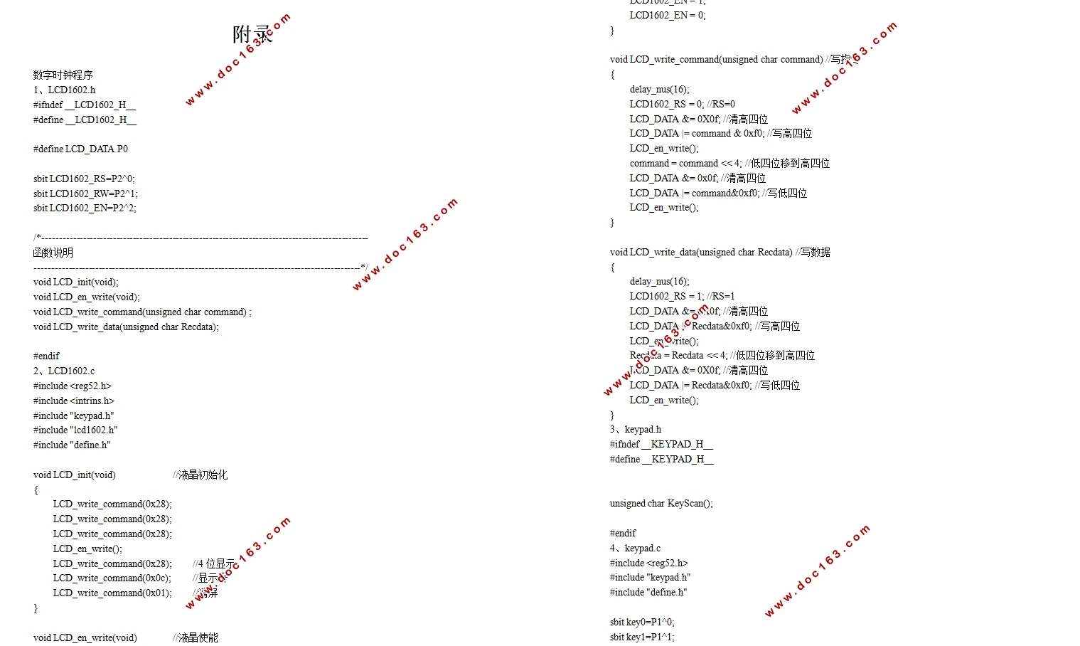
附录 34
[资料来源:Doc163.com]